SEMI106 Flexible Hybrid Electronics 2.0 based on Fan-Out Wafer Packaging
Course Description
This course will help you learn why and how new packaging paradigms like chiplets and dielets impact the world of flexible hybrid electronics (FHE) from one of the industry's foremost experts, Dr. Subramanian Lyer of UCLA. This course explores how these packages pack such a punch, enabling advanced performance in a much smaller and more flexible footprint.
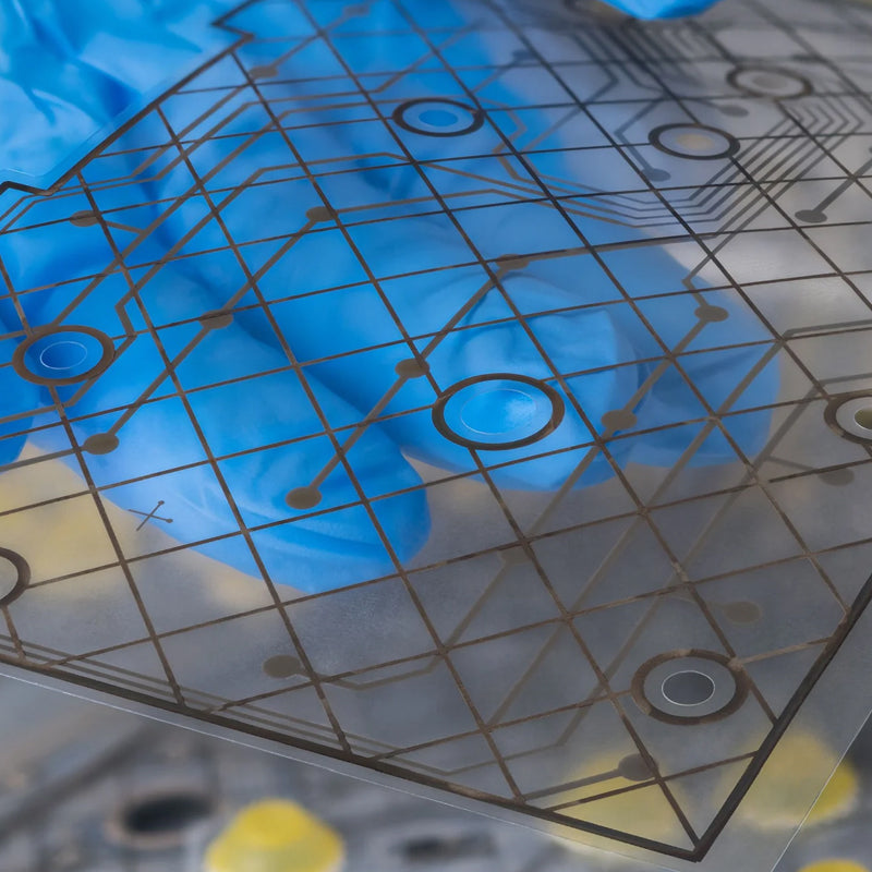
The area of Flexible Hybrid Electronics (FHE) has also developed and is making a significant impact in the area of medical wellness electronics. The first generation of these devices have, for the most part adapted Printed Circuit Board (PCB) technology by using thinner PCB's and assembling either thinned or thin packaged older generation chips onto these platforms, typically with coarse printed wiring to connect a small number of such chips. This approach while immensely useful to get the field going, needs to be adapted and borrowed from both silicon and advanced packaging technology trends, so that we can advance this trend to the next level. The key paradigm challenges ahead are scaling FHE in general which includes the adoption of dielet (chiplet) technology in more advanced CMOS nodes including edge-AI, higher performance interconnects, flexible high-density energy storage, wireless communication and advanced ergonomics all at a lower cost and higher reliability.
Course Objectives
- Learn about the challenges and outline a possible technology roadmap to achieve goals associated with scaling FHE, including the adoption of dielet (chiplet) technology in more advanced CMOS nodes, including edge-AI
Course Duration
45 minutes
Target Audience
Managers, supervisors, engineers, technicians or any individual working directly with this equipment or product
Requisite Knowledge
None
This product has no reviews yet.